📘 ATOMERA INC (ATOM) — Investment Overview
🧩 Business Model Overview
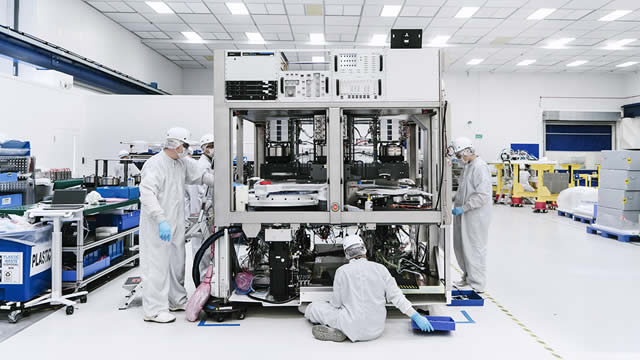
Atomera develops and commercializes materials/process IP intended to improve semiconductor device performance and reliability. The company’s value proposition is not a product sold like a consumable commodity, but a set of technical know-how that can be integrated into wafer fabrication flows—typically at interface layers where device reliability and leakage behavior are most sensitive.
In practice, the economic model depends on (1) getting qualified by advanced-node manufacturers (foundries and IDMs), (2) embedding the process into production manufacturing recipes, and (3) converting engineering access into monetization through licensing economics (upfront/milestone payments) and/or downstream royalty streams tied to adoption volume.
💰 Revenue Streams & Monetisation Model
Atomera’s monetization framework is best viewed as a staged pathway from R&D and customer development to commercialization:
- Licensing and development revenue: milestone-style payments tied to technical validation and customer qualification work.
- Royalty-like recurring economics: once processes are adopted in production, value can scale with device/manufacturing throughput, creating longer-duration revenue visibility than pure one-time R&D.
- Project-based services (where applicable): engineering support to help integrate the process into customer manufacturing flows.
Margin structure is typically characterized by low incremental cost after platform/process maturity, but with meaningful upfront technical and customer-qualification spend. The primary margin driver is successful conversion from feasibility work to scaled manufacturing adoption, which shifts revenue mix from project-based to adoption-linked economics.
🧠 Competitive Advantages & Market Positioning
Moat thesis (hard-to-replicate): Atomera’s competitive advantage is driven by manufacturing integration and qualification switching costs plus intellectual property in process/material engineering.
- High switching costs (qualification + integration): Advanced-node process changes require extensive verification across reliability, yield, and manufacturability. Once a fab qualifies a specific process stack, the cost of switching to a substitute material/process is high (technical risk, engineering time, and yield impact).
- Intangible assets (IP + know-how): Proprietary process concepts and associated IP create a barrier that is difficult to copy without replicating the enabling engineering details and achieving comparable device-level results.
- Customer stickiness (multi-year roadmaps): Semiconductor technology roadmaps extend across design and manufacturing cycles, encouraging longer-term collaborations with suppliers who can demonstrate device reliability improvements that matter to large manufacturing customers.
Competitive benchmarking (substitutes and alternatives):
- Applied Materials (process equipment and materials processing enablement): competes indirectly by offering platforms and process capabilities that customers may use to pursue alternate reliability solutions.
- Lam Research (semiconductor process equipment): competes indirectly as part of the broader ecosystem of process integration that can support alternative approaches to thin-film and interface engineering.
- SOITEC (silicon-on-insulator and advanced substrate technologies): competes as an alternative pathway to addressing device scaling constraints through different materials/substrate strategies rather than Atomera’s specific interface/process approach.
Atomera’s differentiation is centered on device interface/process engineering as a targeted reliability/performance improvement layer, whereas the named companies are positioned more broadly across equipment and alternative materials/substrate platforms. That distinction matters because fab customers seek solutions that fit into their existing manufacturing flows with minimal disruption and high reliability performance.
🚀 Multi-Year Growth Drivers
Atomera’s long-run opportunity is tied to persistent semiconductor scaling pressures and the economic need to sustain performance per watt and reliability as device geometries evolve. Over a 5–10 year horizon, growth drivers can be framed as:
- Advanced-node reliability demand: As nodes progress, interface-related reliability degradation and leakage issues become more challenging, increasing the value of targeted process/material improvements.
- Performance-per-watt and yield economics: Manufacturers prioritize solutions that can improve device characteristics without sacrificing yield—making “integration-ready” approaches more valuable than purely theoretical improvements.
- TAM expansion across logic and memory: While adoption can be initially concentrated in specific device structures, comparable reliability challenges can appear across multiple technology platforms, expanding addressable use cases.
- Long qualification cycles favor proven suppliers: Qualification barriers can create a “winner” dynamic: once a process stack is validated, follow-on designs can increase adoption likelihood.
⚠ Risk Factors to Monitor
- Qualification and ramp risk: Even with technical promise, conversion from development to production adoption can be slow and uncertain due to yield, reliability, and manufacturability requirements.
- Customer concentration: A small set of fabs/IDMs can drive revenue volatility; delays or changes in roadmap priority can impact commercialization timing.
- Technological substitution: Alternative reliability approaches—whether equipment-driven process changes, different materials stacks, or substrate strategies—can reduce the incremental value of Atomera’s approach.
- Capital and execution intensity: Semiconductor process integration and customer qualification require sustained engineering effort and working capital.
- IP defensibility and licensing structure: The economic outcome depends on the durability of IP positions and the enforceability of licensing economics.
📊 Valuation & Market View
The market often values platform-style semiconductor enabling companies using a mixture of forward revenue potential and event-driven milestones, with emphasis on adoption probabilities rather than near-term operating profitability.
- Revenue multiple frameworks: Early-stage and commercialization-stage companies are frequently discussed in terms of EV/Revenue (or Sales) when royalty/licensing ramps are expected.
- Key valuation drivers: evidence of customer qualification progress, quality and durability of royalty-like economics, and repeatable adoption across multiple node transitions or product families.
- Risk discounting: valuation typically reflects long cycle times and binary aspects of adoption—progress indicators can matter as much as absolute financial performance in the short run.
🔍 Investment Takeaway
Atomera’s investment case rests on whether its interface/process engineering platform can achieve sustained adoption in advanced semiconductor manufacturing. The strongest structural moat is not scale in the conventional sense, but qualification-driven switching costs paired with proprietary process/material IP. If the company can convert customer validation work into durable licensing/royalty economics across technology roadmaps, the business can develop long-duration revenue characteristics supported by semiconductor reliability demand.
⚠ AI-generated — informational only. Validate using filings before investing.